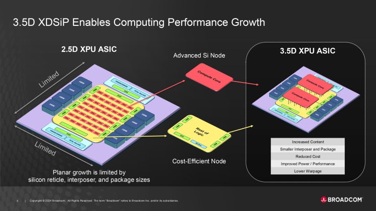
Broadcom has revealed its “cutting edge” 3.5D XDSiP platform technology, focused on custom compute platforms to deliver significant gains in performance and efficiency.
Broadcom’s Latest XDSiP 3.5D Platform Enables AI XPU at Scale, Focusing on AI and HPC Workloads
(Press release): Broadcom Inc. today announced the availability of its 3.5D eXtreme Dimension System in Package (XDSiP) platform technology, enabling mainstream AI customers to develop next-generation custom accelerators (XPUs). The 3.5D Broadcom has reached a significant milestone by developing and launching the industry’s first 3.5D Face-to-Face (F2F) XPU.
The immense computing power required for training generative AI models relies on massive clusters of 100,000 scaling up to 1 million XPUs. These XPUs require increasingly sophisticated integration of compute, memory, and I/O capabilities to achieve the necessary performance while minimizing power consumption and costs. Traditional methods such as Moore’s Law and process scaling struggle to meet these requirements. Therefore, advanced system-in-package (SiP) integration becomes crucial for next-generation XPUs.

Over the past decade, 2.5D integration, which involves the integration of multiple chipsets up to 2500mm² silicon and HBM modules up to 8 HBMs on an interposer, has proven valuable for development from XPU. However, as new and more complex LLMs are introduced, their training requires 3D silicon stacking for better size, power, and cost. Therefore, 3.5D integration, which combines 3D silicon stacking with 2.5D packaging, is poised to become the technology of choice for next-generation XPUs in the coming decade.
Broadcom’s 3.5D XDSiP platform provides significant improvements in interconnection density and energy efficiency compared to the Face-to-Back (F2B) approach. This innovative F2F stack directly connects the top metal layers of the top and bottom die, providing a dense, reliable connection with minimal electrical interference and exceptional mechanical strength. Broadcom’s 3.5D platform includes an IP and proprietary design flow for efficient patch-by-build 3D chip stacking for power, clock and signal interconnects.
Key Benefits of Broadcom’s XDSiP 3.5D
- Improved interconnection density: Achieves 7x higher signal density between stacked chips compared to F2B technology.
- Superior energy efficiency: Delivers a 10x reduction in power consumption in die-to-die interfaces using 3D HCB instead of planar die-to-die PHYs.
- Reduced latency: Minimizes latency between compute, memory, and I/O components within the 3D stack.
- Compact form factor: Allows for smaller interposers and package sizes, resulting in cost savings and improved package warpage.
Broadcom’s flagship 3.5D F2F XPU integrates four compute chips, one I/O chip and six HBM modules, leveraging TSMC’s cutting-edge process nodes and 2.5D CoWoS packaging technologies. Broadcom’s proprietary design flow and automation methodology, based on industry-standard tools, ensured immediate success despite the immense complexity of the chip.

The 3.5D XDSiP demonstrated comprehensive functionality and exceptional performance on critical IP blocks including high-speed SerDes, HBM memory interfaces and die-to-die interconnects. This achievement highlights Broadcom’s expertise in the design and testing of complex 3.5D integrated circuits.
TSMC and Broadcom have worked closely over the past several years to bring together TSMC’s most advanced logic processes and 3D chip stacking technologies with Broadcom’s design expertise.
We look forward to producing this platform to unlock AI innovations and enable future growth.
– Dr. Kevin Zhang, Vice President of Business Development and Global Sales and Deputy Co-COO, TSMC
With more than five 3.5D products in development, the majority of Broadcom’s consumer AI customers have adopted the 3.5D XDSiP platform technology with production deliveries beginning in February 2026. For more information on the platform Custom 3.5D Computing Software from Broadcom, please click here.


